-
Scientists grow wrinkle patterns on polymer surfaces in a spontaneous and reversible manner, spurring advances in smart soft matter technologyNatural creases on animal skin have inspired the engineering of such patterns on polymers for the design of “smart surfaces.” However, the engineered patterns are often permanent, limiting their control. In their latest study, scientists from Ajou University, Korea, have come up with a way to form wrinkles on hydrogel surfaces in a controlled, reversible fashion, opening doors to innovations in soft-matter-based smart technology. Fabrication of polymer films with long-range wrinkle patterns can aid in the development of smart surfaces with applications in dry adhesion, sensing, and smart windows. A new study in Advanced Materials Interfaces reveals a way to control wrinkle formation in soft matter.Photo Courtesy: Advanced Materials Interfaces, Wiley Online Library Sometimes, simply looking at nature can inspire clever innovations in technology. In fact, an entire field of research, called “biomimetics,” is based on the idea of emulating nature to engineer novel structures like “smart surfaces,” which can change their shape or property in response to changes in the ambient environment (temperature, humidity, light intensity, pH, etc.)An inspiration for these smart surfaces comes from the crinkles or crease patterns found on the skin of animals. “The wrinkles on our skin are designed for practical purposes such as gripping objects without slipping or facilitating heat dissipation through a large surface area. In addition, they can be used to control alignment of small particles on a material surface without needing a complex chemical or physical interaction,” explains Dr. Tae Soup Shim from Ajou University, Korea, whose research group focuses on the design of smart surface materials. While such wrinkle patterns have been successfully engineered in polymeric materials, their precise control has been challenging due to the fact that such structures are often permanent. Now, in a new study published in Advanced Materials Interfaces, Dr. Shim and his colleagues found a way to format uniform wrinkle structures. In their design, they successfully formed crease patterns on a hydrogel (a crosslinking chain of “water-loving” polymers) film from its surface deformations, in a uniform manner. Dr. Shim says, “Through our study, we were able to control the wrinkle formation mechanism step by step, for the first time.”In their strategy, the scientists used a technique called “reaction-diffusion-mediated photopolymerization” (RDP) (essentially a UV-light-mediated polymerization reaction) to fabricate a hydrogel film called p(HEMA-co-AA) film, and then caused it to deform, giving rise to hill-and-valley-type structures. Depending on the properties of the UV light used, the structures could be either isotropic (with the same properties in all directions) or anisotropic (properties changing with direction). The scientists found that the anisotropic structures were the key to controlling the wrinkle formation process, and thus, they used a UV source with an anisotropic intensity profile to generate anisotropic hills and valleys. Then, the scientists increased the pH of the film, which caused it to swell and form the crease patterns. Since the swelling process is reversible, scientists could repeat the creasing and flattening of the film simply by changing the pH!Further, to demonstrate the aligning behavior of particles due to the crease patterns, scientists made the film interact with “free-moving” yeast cells. They noticed that as the creases developed, not only did the yeast cells align themselves along the crease patterns but also reproduced along them, showing guided cell growth. The p(HEMA-co-AA) film could, therefore, potentially serve as a suitable platform for studying other direction-specific cells and biomolecules, such as neurons and DNA. With such promising results, scientists are excited about the potential applications of wrinkle structures in real life. “We expect that the strategy implemented in our study will make the fabrication of polymer materials with a uniform wrinkle structure much easier. These polymers can then be used to design smart surface materials that can find applications in smart adhesion technology, gas sensing, and smart windows,” comments Prof. Shim. This study, indeed, adds a new wrinkle in the development of smart materials!ReferenceAuthors:Mina Kim1, Kwon-Young Choi2, Ju Min Kim1,3 and Tae Soup Shim1,3Title of original paper:Stepwise Evolution of Crease Patterns on Stimuli-Responsive Hydrogels for the Production of Long-Range Ordered StructuresJournal:Advanced Materials InterfacesDOI:10.1002/admi.202001551 Affiliations:1Department of Energy Systems Research, Ajou University 2Department of Environmental Engineering, Ajou University3Department of Chemical Engineering, Ajou University*Corresponding author’s email: tsshim@ajou.ac.kr About Ajou UniversityFounded in 1973, Ajou University has quickly grown to become one of the top universities in the Republic of Korea. With over 15,000 students and 50 research centers in diverse fields, Ajou University partakes in the largest national research and graduate education project funded by the Korean Ministry of Education. In line with its recently reformed vision, Ajou University’s goal is to change society by connecting minds and carrying out high-impact research to improve the welfare of people in and outside Korea. Website: https://www.ajou.ac.kr/en/index.do About the authorDr. Tae Soup Shim is an Associate Professor at the Departments of Chemical Engineering and Energy Systems Research, Ajou University, Korea. He received a PhD degree in Chemical and Biomolecular Engineering from KAIST, Korea. Following this, he worked as a postdoctoral researcher at Department of Chemical and Biomolecular Engineering, University of Pennsylvania, USA. His major research interests include colloidal self-assembly, stimuli-responsive materials, interfacial phenomena, and biomimetics. Currently, his group has been focusing on designing micro-/nanostructures based on soft matter for the development of shape-transformable soft actuators, flexible electronic devices, and smart surface materials.
-
23
- 작성자OI***
- 작성일2021-02-10
- 3698
- 동영상동영상
-
A breakthrough in 2D graphene fabrication paves the way for its large-scale production Graphene is a promising pure carbon 2D material that can revolutionize electronics. However, it is difficult to produce high-quality large-area graphene films. Now, scientists from Korea have developed a novel method to peel off uniform and atomically thin layers of graphene from a natural graphite crystal, paving the way for large-scale production. Graphene is a promising nanomaterial that could lead to tremendous advances in electronics, including bendable and wearable devices, faster transistors, and new semiconductors Photo courtesy: Shutterstock Graphene is a solid made purely from carbon atoms arranged in a 2D honeycomb-like structure. Its unique mechanical, chemical, electric, and optical properties have made it a hot topic in materials science; the next generation of electronics like faster transistors, wearable and bendable phones and other electronics can very well be based on graphene. Unfortunately, there are still no efficient ways to produce large-area graphene films with a thickness of a few atoms. If graphene is to revolutionize upcoming technology, a better fabrication technique is a must. That’s why a team of scientists from Korea, led by Associate Professor Jae-Hyun Lee from Ajou University, recently published a study in Science Advances in which they pioneer a promising strategy to produce atomically thin graphene films. Instead of going for a chemical route, they focused on developing a new method for the exfoliation—or peeling off—of graphene out of a natural graphite crystal. Traditional exfoliation methods involve removing thin layers of graphene from graphite using special adhesive tapes. However, this only yields pieces of graphene a few micrometers across. In the new strategy the scientists developed, a thin metallic film is first deposited on a large graphite crystal and then removed, lifting along a graphene film from the crystal. The key to this method is that the metallic film attracts carbon atoms in the top few layers with a slightly higher binding energy than carbon atoms in deeper layers. What’s more, different metals can yield large graphene layers with a uniform thickness of one, two, or three carbon atoms. “We studied the mechanisms by which cracks form when graphene is exfoliated and found a way to control them in size and direction at an atomic scale,” remarks Dr. Lee, “The area and density of the atomically thin graphene layers we extracted were respectively 4,200 and 6,000 times larger compared with existing exfoliation methods.” This study could solve the long-standing issue of producing high quality graphene films with high yield and large area, which has been an obstacle to the research and commercialization of graphene-based technology. Excited about the results, Dr. Lee concludes, “Graphene may bring forth a new generation of electronics, including faster transistors and even wearable and bendable phones. Our exfoliation technique paves the way for developing manufacturing process for the mass production of graphene and other 2D materials.” With any luck, refining this technique could set us on the course for a technological revolution! ReferenceAuthors:Ji-Yun Moon1, Minsoo Kim2, Seung-Il Kim1, Shuigang Xu2, Jun-Hui Choi3, Dongmok Whang4, Kenji Watanabe5, Takashi Taniguchi6, Dong Seop Park7, Juyeon Seo7, Sung Ho Cho7,*, Seok-Kyun Son3,* and Jae-Hyun Lee1,*Title of original paper:Layer-engineered large-area exfoliation of grapheneJournal:Science AdvancesDOI:10.1126/sciadv.abc6601Affiliations:1Department of Energy Systems Research and Department of Materials Science and Engineering, Ajou University2School of Physics and Astronomy, University of Manchester3Department of Physics, Mokpo National University4School of Advanced Materials Science and Engineering, Sungkyunkwan University5Research Center for Functional Materials, National Institute for Materials Science6International Center for Materials Nanoarchitectonics, National Institute for Materials Science7Mobile Display Process Architecture, Samsung Display*Corresponding authors’ emails: jaehyunlee@ajou.ac.kr (J.-H.L.)About Ajou UniversityFounded in 1973, Ajou University has quickly grown to become one of the top universities in the Republic of Korea. With over 15,000 students and 50 research centers in diverse fields, Ajou University partakes in the largest national research and graduate education project funded by the Korean Ministry of Education. In line with its recently reformed vision, Ajou University’s goal is to change society by connecting minds and carrying out high-impact research to improve the welfare of people in and outside Korea. Website: https://www.ajou.ac.kr/en/index.do About the authorDr. Jae-Hyun Lee is an Associate Professor at the Department of Energy Systems and Engineering at Ajou University, Korea. His group explores and develops new physics and phenomena using advanced two-dimensional (2D) materials. The particular speciality of his group is the mesoscopic investigation of new types of van der Waals (vdW) heterostructures, including carbon nanotubes, 2D materials, and nanowires.
-
21
- 작성자OI***
- 작성일2021-02-08
- 6916
- 동영상동영상
-
The NRF2 gene is known to be a cancer suppressor, but perhaps “it is two-faced,” scientists say, paving the way for better cancer research and treatment The NRF2 gene has been traditionally believed to suppress cancer with its antioxidant properties. However, recent cancer genome analyses suggest that NRF2 activation may, in fact, promote several cancers, including those of the lungs. In a new study, an international joint research team, including Korean scientists, finds evidence of this in mouse models of lung cancer and in data from two large clinical trials. Their findings can help understand cancer better, guiding us towards more effective therapies. Lung cancer is a leading cause of cancer deaths worldwide, but extensive research is yet to yield a sufficiently effective treatment option. However, now an international research group including scientists from Korea may just have stumbled upon a solution. Photo Courtesy: ShutterstockLung cancer is one of the most dreaded cancers today, given its massively high mortality rate. But while scientists have been trying to find a cure for decades, their efforts have met with little success. “I believe this is because we still don’t understand cancer correctly or fully,” says Prof. Sang-Min Jeon from Ajou University, Korea, who has been researching the roots of cancer. “I think that cancer originates in the microenvironment where toxins are accumulated such that cells that are able to utilize such toxins as nutrients proliferate and become cancerous.” Led by this belief, Prof. Jeon has recently turned to genes involved in the metabolism of toxins called reactive oxygen species (ROS)—free radicals or unstable atoms that can damage cells with their high reactivity. One such gene is NRF2, which, when activated, is believed to suppress cancer by reducing ROS. However, recent studies have detected aberrant activation of NRF2 in certain lung cancers, raising the possibility that it may be an “oncogene”—one that helps cause cancer—rather than a “cancer suppressor” gene. In their new study published in Clinical Cancer Research, Prof. Jeon and his international team of scientists confirm this possibility. In their study, Prof. Jeon and team took genetically modified mice with lung cancer and set out to check for NRF2 mutation. They found aberrant activation of NRF2 and saw that it assists other oncogenes in promoting the cancer, leading to decreased survival, despite reducing ROS toxicity. The team also analyzed the results of two large-scale human clinical trials, OAK and IMpower 131. Patients with an aberrantly active NRF2 showed poorer response to chemotherapy and immunotherapy and, therefore, had poorer prognosis and a significantly lower survival rate than those without NRF2 activation.Based on these findings, Prof. Jeon believes NRF2 inhibitors have great potential as therapeutic approaches for lung cancer. “As a next step, we have set up a biotech company called SCL Therapeutics where we are developing first-in-class NRF2 inhibitor drugs for cancer therapy. We are currently actively conducting preclinical trails”, he says. This study does provide remarkable insights into the driving mechanisms of lung cancer. Perhaps, Prof. Jeon’s hopes will translate to a revolutionary new therapy in the near future, and lung cancer will not be so dreadful after all. ReferenceAuthors:Anju Singh1, Anneleen Daemen2, Dorothee Nickles2, Sang-Min Jeon3,4, Oded Foreman5, Kuladeep Sudini1, Florian Gnad2, Stephane Lajoie1, Naina Gour1, Wayne Mitzner1, Samit Chatterjee1, Eun-Ji Choi4, Buvana Ravishankar6, Amy Rappaport7, Namrata Patil8, Mark McCleland8, Leisa Johnson7, George Acquaah-Mensah9, Edward Gabrielson10, Shyam Biswal1 and Georgia Hatzivassiliou3Title of original paper:NRF2 activation promotes aggressive lung cancer and associates with poor clinical outcomesJournal:Clinical Cancer Research DOI:10.1158/1078-0432.CCR-20-1985Affiliations:1Department of Environmental Health Science and Engineering, Johns Hopkins University School of Public Health 2Oncology Bioinformatics, Genentech Inc.3Translational Oncology, Genentech Inc.4College of Pharmacy and Research Institute of Pharmaceutical Science and Technology, Ajou University5Pathology, Genentech Inc.6Cancer Immunology, Genentech Inc.7Disocvery Oncology, Genentech Inc.8Oncology Biomarker Development, Genentech Inc.9Department of Pharmaceutical Sciences, Massachusetts College of Pharmacy and Health Sciences10Department of Pathology and Oncology, School of Medicine, Johns Hopkins University *Corresponding authors’ email: anneleen.daemen@gmail.com, nicklesd@gene.com, sbiswal@jhu.edu About Ajou UniversityFounded in 1973, Ajou University has quickly grown to become one of the top universities in the Republic of Korea. With over 15,000 students and 50 research centers in diverse fields, Ajou University partakes in the largest national research and graduate education project funded by the Korean Ministry of Education. In line with its recently reformed vision, Ajou University’s goal is to change society by connecting minds and carrying out high-impact research to improve the welfare of people in and outside Korea. Website: https://www.ajou.ac.kr/en/index.do About the authorSang-Min Jeon is an Associate Professor in the Department of Pharmacy at Ajou University. He is currently involved in cancer research to uncover the origin of cancer from a unique microenvironment-metabolism perspective. His goal is to develop innovative anti-cancer strategies based on the underlying causes of cancer. He is also engaged in the development new anti-cancer drugs through a biotech company that he has recently co-founded. Before coming to Ajou University, he completed his postdoctoral training at the Translational Oncology lab at Genentech Inc. in California, USA. In 2011, he received his PhD in Biochemistry and Molecular Genetics from the Chicago College of Medicine, University of Illinois, USA.
-
19
- 작성자OI***
- 작성일2021-02-05
- 3969
- 동영상동영상
-
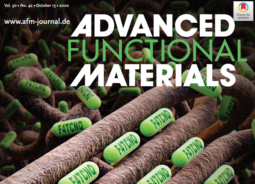
New hybrid strategy could unlock the use of organic compounds to convert body heat into electricity for portable devicesAlthough conjugated polymers are promising materials for many electronic applications, increasing their conductivity enough for efficiently converting heat to electricity has been tricky. Now, scientists from Ajou University, Korea, have devised a hybrid strategy that combines two existing doping methods to obtain unprecedented results. This could unlock the use of these polymers to power portable electronic devices and sensors using body heat.Thermoelectric conversion is a highly popular unconventional energy harvesting technique; theoretically, it allows for powering portable electronic devices and sensors using nothing but body heat. Many researchers have high hopes on conjugated polymers (CPs), special arrangements of long organic molecules that are used in flexible electronics, transistors, and solar cells. However, there are no effective methods to make CPs conductive enough for high efficiency thermoelectric energy conversion. Scientists at Ajou University, Korea, have recently pioneered a novel strategy that demonstrates extremely promising results. In their study, featured on the front cover of the latest issue of Advanced Functional Materials (Volume30, Issue42 2004598), they combined two of the best known methods for enhancing the conductivity of CPs into “hybrid doping”. This image, selected as the cover for Advanced Functional Materials, shows long strands of conjugated polymers doped to the max with F4TCNQ, a standard organic dopant Photo courtesy: Wiley Online Library In materials science, doping is the process of intentionally adding impurities to a material to enhance certain properties. For CPs, existing doping methods are “mixture blending” and “sequential doping.” In mixture blending, the polymer and the dopant are mixed in a solution, which is then spin coated to produce the doped CP. However, the amount of dopant that can be safely used without compromising the polymer structure is very small. Sequential doping, meanwhile, involves spin coating the CP first and then dipping it into a dopant solution. With this approach, the dopant can only penetrate the layers of the polymer at amorphous regions, leaving the crystalline areas undoped.The combined strategy is a straightforward fusion of both techniques; a pre-doped CP produced through mixture blending is dipped into a dopant solution. “Hybridizing both processes effectively maximizes the degree of doping of the CPs, yielding maximum conductivity without sacrificing other properties,” Professor Jong. H. Kim, who led the study, explains. The scientists compared CPs produced using each method in terms of their microscopic structure, optoelectrical properties, stability, and thermal conversion performance; the CPs processed with hybrid doping came out on top in all relevant areas. Excited about the results, Professor Kim comments: “Hybrid doping let us optimize the thermal energy conversion efficiency of existing and new CPs. In turn, this will eventually allow us to harvest waste heat from various sources, including the human body, to power all types of portable electronic devices and Internet-of-Things sensors.” This study is a huge step in the development of eco-friendly functional materials, and highly doped CPs will surely find their way into the electronic devices of tomorrow.ReferenceAuthors:Sang Eun Yoon1, Yeongkwon Kang2, Gyeong G. Jeon1, Dohyeon Jeon3, Sang Yeon Lee4, Seo-Jin Ko5, Taekyeong Kim3, Hyungtak Seo4, Bong-Gi Kim2, and Jong H. Kim1*Title of original paper:Exploring Wholly Doped Conjugated Polymer Films Based on Hybrid Doping: Strategic Approach for Optimizing Electrical Conductivity and Related Thermoelectric PropertiesJournal:Advanced Functional MaterialsDOI:10.1002/adfm.202004598Affiliations:1Department of Molecular Science and Technology, Ajou University2Department of Organic and Nano System Engineering, Konkuk University 3Department of Physics, Hankuk University of Foreign Studies4Department of Materials Science and Engineering and Department of Energy Systems Research, Ajou University5Division of Advanced Materials, Korea Research Institute of Chemical Technology*Corresponding author’s email: jonghkim@ajou.ac.kr About Ajou UniversityFounded in 1973, Ajou University has quickly grown to become one of the top universities in the Republic of Korea. With over 15,000 students and 50 research centers in diverse fields, Ajou University partakes in the largest national research and graduate education project funded by the Korean Ministry of Education. In line with its recently reformed vision, Ajou University’s goal is to change society by connecting minds and carrying out high-impact research to improve the welfare of people in and outside Korea. Website: https://www.ajou.ac.kr/en/index.do About the authorJong H. Kim (Jong Hyun Kim) is an Associate Professor of the Department of Molecular Science and Technology and the Department of Applied Chemistry and Biological Engineering at Ajou University. His group is developing new approaches to fabricate high-efficiency energy harvesting devices, including thermoelectric and photovoltaic devices. Professor Kim’s research group is also developing high-efficiency doping processes for transparent and stretchable electrodes for solar cells and NIR photodetectors. Before joining Ajou University, Jong H. Kim completed his postdoctoral training at Alex K.-Y. Jen’s lab at the University of Washington, USA. In 2011, he received a PhD in the Department of Materials Science and Engineering from Seoul National University, Korea.
-
17
- 작성자국제협력팀
- 작성일2021-02-03
- 3453
- 동영상동영상
-
A team of researchers including Ajou University’s Prof. Seo Hyung-tak has successfully developed an integrated optoelectronic diode capable of adapting, in a fashion similar to human visual perception, to various environments. The team’s discovery is expected to help develop visual devices with artificial nerves, intelligent photosensors, data processors, and innovations in robotics.Prof. Seo (Dept. of Materials Science and Engineering / Graduate Dept. of Energy Systems, pictured) has announced that his team has developed a photosensor diode capable of differentiating information processing depending on angles of perception. The team’s invention is discussed in detail in “Environment-Adaptable Photonic-Electronic Coupled Angular Perception System,” published in the October issue of ACS Nano (IF = 14.588). The team included two other members from Ajou: Prof. Kim Sang-wan (Dept. of Electrical and Computer Engineering) and Dr. Mohit Kumar (lead author).The human vision system is capable of adapting on its own to changes in its surroundings, including differences in lighting, by detecting changes in optic signals in real time. It is also capable of differentiating between visual signals from different angles of vision (up or down, left or right) and processing the obtained data accordingly. Human vision captures optical data and converts it into photoelectronic signals, which are then encoded into electric spikes of appropriate sizes. Information thus processed is then transmitted to the visual cortex and stored on the synaptic network.Numerous attempts have been made so far to develop artificial sight by simulating the complex and intricate workings of human visual perception. Success has been elusive so far, however, in developing artificial vision with a sufficiently simple structure and a rational energy demand.Much of the research on artificial sight circuits to date has focused on understanding and visualizing information under general lighting. Effective artificial sight, however, crucially requires a technology capable of recognizing objects from wide viewing angles. Only on the basis of angular perception can researchers proceed to develop an effective and simple humanoid photoelectronic circuit capable of replacing the excessively complex circuits that exist today. Moreover, simplifying these complex circuits requires memory storage capable of adapting automatically to diverse environments.Prof. Seo’s team has created a photosensitive semiconductor capable of adapting to changing environments and simulating the human nervous system by first creating a quality titanium dioxide (TiOs) nanofilm and then evenly arranging a silver nanowire on it. The silver nanowire (NW) maximizes the photoelectronic effect on angular visual perception, enabling the semiconductor to perceive and process visual data across a wide angle (± 70º). The Schottky-style combination of the silver nanowire and titanium dioxide also ensures the effective collection of photoelectrons to enhance sensitivity to photonic (ultraviolet) signals. This diode structure is simple, yet effectively simulates human visual perception.Using a 3x3 array, Prof. Seo’s team has created a visual perception diode whose circuit can itself recognize objects in diverse environments. The team has thus discovered that, even for the same given patterns of optic signals, the intensity and duration of memory of those signals vary depending on the given visual angles, the intensity of given light, and the duration and intervals of optic signals. The team, in other words, has demonstrated that their semiconductor is capable of working in much the same manner as the human visual nerves and cortex, and that the mechanism of their neuromorphic optic signal storage is based on the accumulation and loss of electric charges, due to photoelectric combination, on their Schottky diode.This means that the time it takes for memory stored in the titanium dioxide semiconductor to disappear varies depending on differences in the amounts of light absorbed by the semiconductor because those differences in lighting mean the creation of different amounts of light-induced charges (electron-hole pairs). With this invention, the same in-vivo memory-oblivion system can be added to the memory used to sense and store images on devices such as smartphones.Prof. Seo commented, “Artificial sight diodes require many component technologies. Our recent study is significant in that it demonstrates how a transparent semiconductor, capable of adapting to changes in environments and detecting and processing optic signals with relatively little energy, can be created.”He also expects the new diode to “have a wide variety of applications, including intelligent photosensors, data processing, and robotics.”The study has been made possible thanks to support from the Future New Material and Original Technology Development Program and the Basic Research Support Program for Experienced Basic Researchers, co-organized by the Ministry of Science and ICT and the National Research Foundation of Korea.
-
15
- 작성자OI***
- 작성일2020-12-28
- 4366
- 동영상동영상