- About Ajou
- Admission
- Academics
-
Research
Research
-
International
International
- Campus Life
-
News and Event
News and Event
- AUT
Ajou News
NEW Prof. Ilkwon Oh’s Research Team Develops AS-ALD Technology for Semiconductor Miniaturization
- 2025-05-02
- 31
- Area-Selective Atomic Layer Deposition (AS-ALD) Gains Attention as a Key Breakthrough Technology
- Enables Patterning Without Exclusive 'EUV Equipment', Allowing for Customized Fabrication
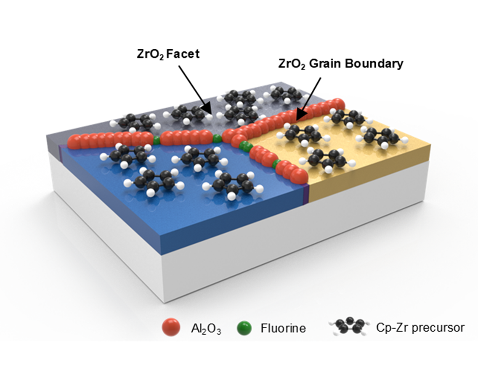
* Caption for the image above: An illustration showing the selective formation of red-colored aluminum oxide (Al₂O₃) only at the grain boundaries — the leakage current pathways — of zirconium dioxide (ZrO₂) through the new area-selective atomic layer deposition (AS-ALD) process developed by the Ajou University joint research team.
This technology is expected to maximize storage capacity while minimizing data loss in DRAM devices.
Professor Ilkwon Oh’s research team at Ajou University has developed a technology that enhances the precision of semiconductor processes through area-selective atomic layer deposition (AS-ALD). This advancement is expected to play a crucial role in the manufacturing of next-generation miniaturized and high-density semiconductor devices.
Professor Ilkwon Oh (Department of Intelligent Semiconductor Engineering and Department of Electrical and Computer Engineering) and a joint research team from the Samsung Advanced Institute of Technology (SAIT) announced their successful development of an AS-ALD technology that can significantly improve the precision of thin film deposition in semiconductor fabrication.
Their research was published in the April issue of Advanced Science under the title “Area-Selective Atomic Layer Deposition on Homogeneous Substrate for Next-Generation Electronic Devices.” Minjeong Lee, Byungjun Won, and Youngjin Lim (Master’s students from the Department of Intelligent Semiconductor Engineering at Ajou University) participated as co-first authors, and Professor Ilkwon Oh served as the corresponding author. Dr. Seonghyun Kim and Dr. Jungkyu Song from SAIT also contributed as co-authors.
Area-Selective Atomic Layer Deposition (AS-ALD) is a process that enables deposition to occur only on specific areas of a semiconductor substrate. This technology allows precise application of desired materials to selected locations on the semiconductor surface.
Traditional Atomic Layer Deposition (ALD), widely used in semiconductor processes, forms uniform thin films across the entire substrate. It has been a key technique in the manufacturing of memory devices such as DRAM and NAND flash, as well as non-memory (system) semiconductors.
However, as semiconductor devices continue to shrink and become more densely integrated, there is an increasing demand for selective thin-film deposition to reduce process steps, lower manufacturing costs, minimize error rates, and improve precision and efficiency. Consequently, AS-ALD has emerged as a core next-generation semiconductor processing technology, attracting attention as a breakthrough solution capable of overcoming the technical limits currently facing the semiconductor industry.
By employing AS-ALD, many conventional process steps can be eliminated, dramatically lowering manufacturing costs and the potential for errors. Additionally, AS-ALD enables semiconductor patterning without the need for expensive extreme ultraviolet (EUV) lithography equipment, which has been monopolized by certain companies, further intensifying industrial and academic interest. Furthermore, AS-ALD opens possibilities for customized fabrication of new types of three-dimensional micro-semiconductor devices that are difficult to achieve using traditional techniques and equipment.
Despite these advantages, the implementation of AS-ALD in actual semiconductor mass production has faced significant challenges. Depending on the chemical materials and substrates used, maintaining precise selective deposition has been difficult, and electrical performance degradation has often been observed when applied to real devices.
To overcome these limitations, the Ajou University research team targeted the widely used ZAZ (ZrO₂/Al₂O₃/ZrO₂) capacitor layer structure in DRAM processes. Specifically, they selectively deposited aluminum oxide (Al₂O₃) only at the grain boundaries—the paths where leakage currents typically occur—thereby minimizing unnecessary Al₂O₃ deposition and effectively improving device performance and reliability.
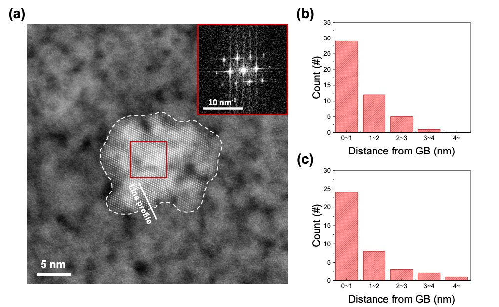
* Transmission electron microscope (TEM) images and chemical composition analysis confirmed the selective formation of Al₂O₃ at grain boundaries.
Graphs b and c illustrate the concentration of Al depending on the distance from the grain boundaries, verifying the selective deposition of Al₂O₃ at the desired locations.
Using zirconium dioxide (ZrO₂) substrates, the research team experimentally analyzed and demonstrated the mechanisms for selective deposition, proving that selective control was feasible. They also confirmed that AS-ALD not only enhances semiconductor device performance but also significantly reduces unwanted leakage currents. This breakthrough suggests a method to maximize storage efficiency in DRAM devices and minimize data loss during device miniaturization, marking an important technical milestone for memory device advancement.
Professor Ilkwon Oh stated, "While area-selective atomic layer deposition is essential for overcoming technological barriers in the semiconductor industry, there have been many challenges in applying it to real processes. Our research experimentally demonstrates that selective deposition and control are achievable, representing a significant advance in semiconductor processing technology."
He added, "We will continue further research to enhance device performance and improve process efficiency for industrial applications."
The Ajou University research team plans to pursue follow-up studies to develop more precise control techniques for atomic layer deposition processes and to explore their industrial applicability.