- About Ajou
- Admission
- Academics
- Research
-
International
International
- Campus Life
-
News and Event
News and Event
-
AUT
AUT
Major Research Result
NEW Extending the Optical Response of Silicon with Broken Symmetry
- 2021-08-26
- 8085
Researchers overcome the fundamental optical limit of silicon-based semiconductors by changing their charge transport behavior with mechanical strain
Optical applications of silicon-based semiconductors are limited to visible and near-infrared wavelengths owing to the fundamental energy band gap in silicon. Now, researchers from Korea have extended the optical limits of silicon crystals utilizing the “flexoelectric effect”, which reduces the band gap, opening doors to novel applications of silicon-based sensors in the wider infrared regime.
Researchers applied a precisely controlled force using a pointed tip to induce strain gradient in a single silicon crystal, breaking its spatial inversion symmetry and extending the infrared response beyond its fundamental limit.
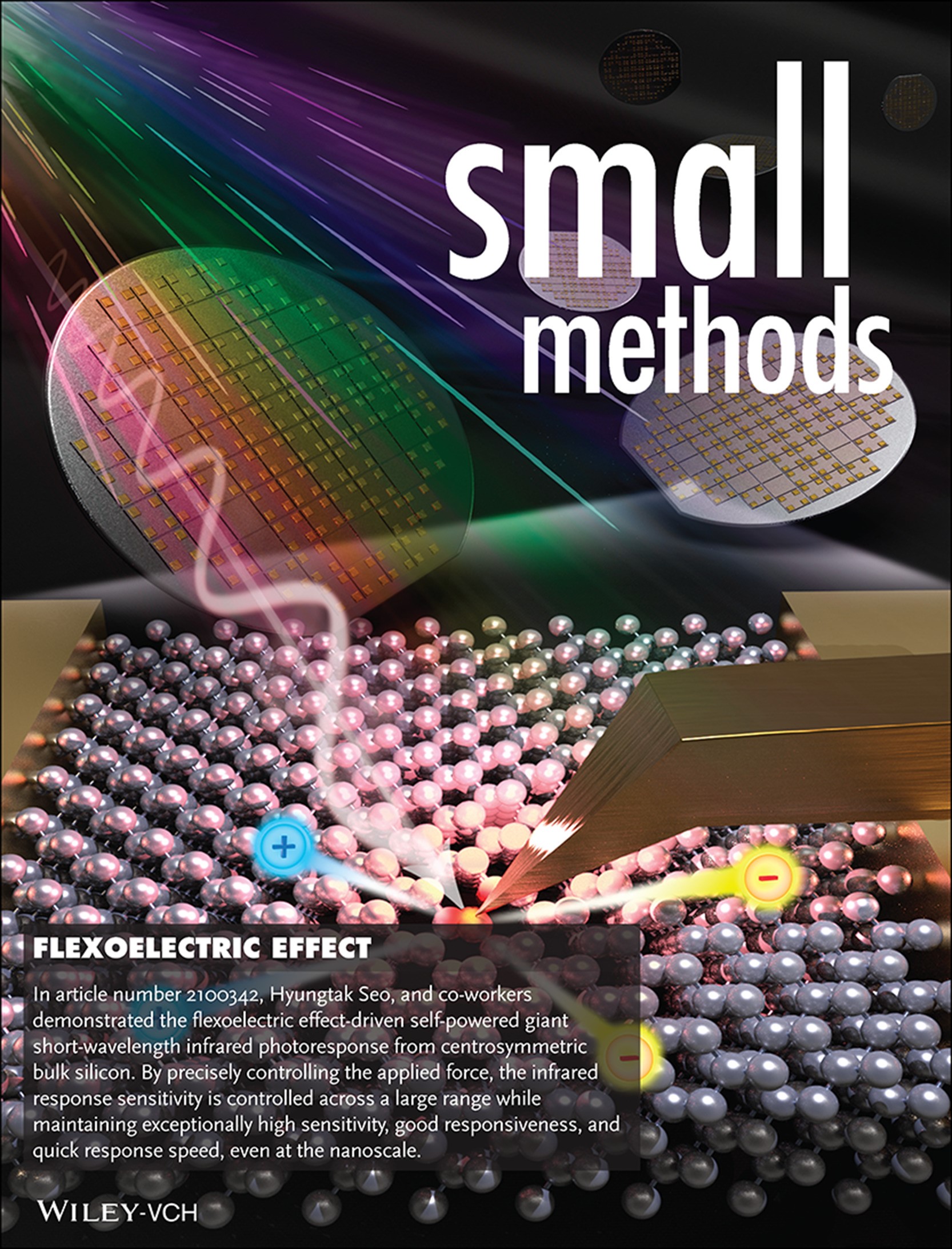
Courtesy: Wiley Online Library
Modern electronics is ruled by silicon. Yet, its potential applications remain limited to the field of optoelectronics because of its fundamental energy gap, which confines its ability to absorb light within a certain wavelength range, limiting optical applications to visible and near-infrared-range devices only. But is there way around this fundamental limit?
In a recent study published in Small Methods, researchers from Ajou University, Republic of Korea, led by Prof. Hyungtak Seo, took up the challenge to reengineer the fundamental energy gap of silicon and extend its usability for infrared applications. In accomplishing this feat, they took the hint from a physical phenomenon called “flexoelectric effect.”
Silicon crystals possess an inherent inversion symmetry which, when broken by applying mechanical strain, gives rise to a spontaneous electric polarization. This, in turn, changes the “effective mass” of the free charge carriers in silicon, modifying its energy gap. When illuminated by light, the strained flexoelectric silicon undergoes a rearrangement in their electronic configuration that alters its fundamental absorption limit, a phenomenon known as the “flexo-photovoltaic effect.”
The researchers took advantage of this response to demonstrate the photon sensing abilities of a single silicon crystal far beyond its fundamental energy gap. Prof. Seo explains, “We extended the sensitivity and responsivity of the silicon crystal to far-infrared wavelengths by introducing an inhomogeneous strain in the crystal using a pointed tip.” Additionally, they conducted photoconductive atomic force microscopic measurements to shed light on the flexoelectric photoresponse of the material and its tunability.
The findings of this breakthrough study open up the possibility of using silicon-based materials for optical applications in the infrared (IR) region. IR photodetectors play a very important role in our day-to-day lives, from process control and exploration in industries to drug and explosive detection at security and defense facilities. Currently, these detectors use gallium/arsenic photosensors, which are expensive and difficult to work with. In contrast, silicon-based sensors are not only highly malleable but also economically viable. “Improving the IR photoresponse of silicon could help us build eco-friendly and cost-effective sensors not only for the industries but also healthcare, transport, and weather monitoring facilities,” comments an optimistic Prof. Seo.
In nature, symmetry may not always be desirable. Sometimes, it needs to be broken!
Reference
Authors: | Mohit Kumar, Jaeseong Lim, Ji-Yong Park, and Hyungtak Seo* |
Title of original paper: | Controllable, Self-Powered, and High-Performance Short- Wavelength Infrared Photodetector Driven by Coupled Flexoelectricity and Strain Effect |
Journal: | Small Methods |
DOI: | 10.1002/smtd.202100342 |
Affiliations: | Department of Energy Systems Research Ajou University, Republic of Korea |
*Corresponding author’s email: hseo@ajou.ac.kr
About Ajou University
Founded in 1973, Ajou University has quickly grown to become one of the top universities in the Republic of Korea. With over 15,000 students and 50 research centers in diverse fields, Ajou University partakes in the largest national research and graduate education project funded by the Korean Ministry of Education. In line with its recently reformed vision, Ajou University’s goal is to change society by connecting minds and carrying out high-impact research to improve the welfare of people in and outside Korea.
Website: https://www.ajou.ac.kr/en/index.do
About Professor Hyungtak Seo
Prof. Hyungtak Seo received a Ph.D. in 2008 from North Carolina State University, USA, and worked at Lawrence Berkeley National Laboratory until September 2011. Since 2011, he has been a Professor at Ajou University, where he is the PI of the Advanced Electronic & Energy Materials (AEEM) Laboratory. His current interests are in (i) fabricating nano-materials for solar cells and photocatalysis applications; (ii) designing materials/devices for next-generation integrated circuit neuromorphic devices; (iii) tuning the electronic properties of nanoscale semiconductors for electrical and energy applications; (iv) and analyzing the properties of functional materials via UPS, XPS, ellipsometry, etc.